Introduction to PCB Manufacturing
Printed Circuit Boards (PCBs) are fundamental components in the world of electronics. These flat boards, made from non-conductive materials like fiberglass, create pathways for electronic circuits by holding and connecting the necessary components. At the core of every electronic device, PCBs enable the functions and communication required for operation. Their significance stretches across numerous industries due to their reliability and efficiency.
The demand for PCBs has been increasing, driven by their essential role in diverse sectors such as consumer electronics, automotive, and telecommunications. Whether in smartphones, automotive control systems, or network equipment, PCBs are integral to the functionalities of these devices. This growing need is reflected in the expansion of the PCB manufacturing market.
The PCB manufacturing process is intricate and involves several stages to ensure the end product meets quality standards. It begins with the design, where detailed schematics are developed, followed by fabrication, wherein the actual boards are constructed from raw materials. Next, assembly puts the components in place, and testing ensures the PCBs function correctly without defects. Each stage is crucial, contributing to the overall performance and reliability of the electronic devices in which these PCBs are installed.
Key Innovations Driving Efficiency in PCB Manufacturing
Automation technologies have revolutionized PCB manufacturing by significantly reducing production times and labor costs. Innovations such as robotic assembly and artificial intelligence (AI) are streamlining processes, allowing for faster throughput and higher accuracy. Robotic arms and AI-powered systems handle repetitive tasks with precision, reducing human error and freeing skilled workers for more complex tasks. This shift not only enhances efficiency but also reduces production costs, making PCB manufacturing more scalable and adaptable to market demands.
Moreover, the development of advanced materials has played a crucial role in enhancing product performance while minimizing size and weight in PCB manufacturing. Flexible PCBs and high-frequency materials offer unique properties, such as better electrical performance and the ability to conform to varying shapes, which are essential in industries like aerospace and wearable technology. These materials contribute to more compact and lightweight devices without sacrificing functionality, aligning with the growing trend toward miniaturization and increased performance standards across various industries.
Incorporating these innovations, PCB manufacturers are not only able to meet current industry demands but are also positioning themselves to adapt seamlessly to future technological advancements. This capacity for innovation ensures competitive advantage in an ever-evolving market landscape, where efficiency and high-performance materials are key elements driving the sector forward.
The Role of Design in PCB Manufacturing
Effective PCB design is critical for minimizing errors and optimizing the performance of electronic devices. A well-thought-out design ensures that components are accurately placed and routed, reducing the likelihood of malfunctions and enhancing the reliability of the final product. As technology evolves, PCB designs must adapt to incorporate smaller, more efficient components without compromising on functionality. For instance, designers must account for the thermal management of increasingly powerful microprocessors and the integration of wireless connectivity options.
Design for Manufacturing (DFM) principles play an essential role in ensuring the manufacturability and cost-effectiveness of PCBs. DFM involves optimizing the layout and selecting components strategically to minimize production challenges and costs. Key considerations include the ease of soldering, the complexity of the design, and the choice of materials that meet performance requirements while remaining affordable. By adhering to DFM principles, manufacturers can achieve a balance between innovative designs and practical production processes, ensuring that products not only perform well but are also economically viable. This focus on design, therefore, not only impacts the immediate quality and functionality of the PCB but also influences long-term production efficiency and profitability.
Quality Control and Testing in PCB Manufacturing
Quality control in PCB manufacturing is vital for ensuring high standards, directly influencing the longevity and reliability of electronic products. A robust quality control system can prevent defects that might lead to product failures, costly recalls, and damage to the manufacturer's reputation. Implementing stringent quality checks at every stage of PCB production is essential for maintaining consistency and meeting customer expectations.
In the realm of PCB manufacturing, several testing methods are commonly employed to ensure product reliability and performance. Automated Optical Inspection (AOI) is one such method, which uses cameras to scan PCBs for defects in solder joints and components. X-ray inspection offers another layer of scrutiny by allowing manufacturers to detect hidden defects, such as those in multilayer or complex PCBs. Functional testing, on the other hand, involves evaluating the PCB in an operating environment to ensure it performs as intended. These testing methods collectively contribute to high-quality PCBs that meet both industry standards and the needs of cutting-edge technological applications.
Products Transforming PCB Manufacturing
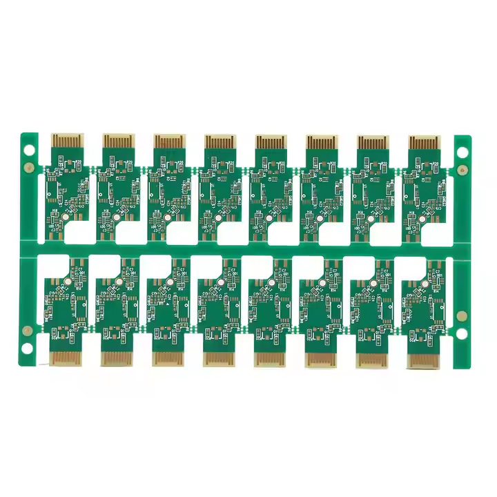
Recent innovations in customized electronics PCBs have significantly enhanced their utility over standard designs. These innovations focus on optimizing conductivity while ensuring precise and accurate component placement within complex electronic systems. Such customization offers advantages like improved signal transmission, minimized electrical issues, and sleek surface finishes, elevating both aesthetic and functional aspects. For instance, the
New arrival Customized Electronics PCB Provider offers flexibility in design necessary to meet diverse application requirements.
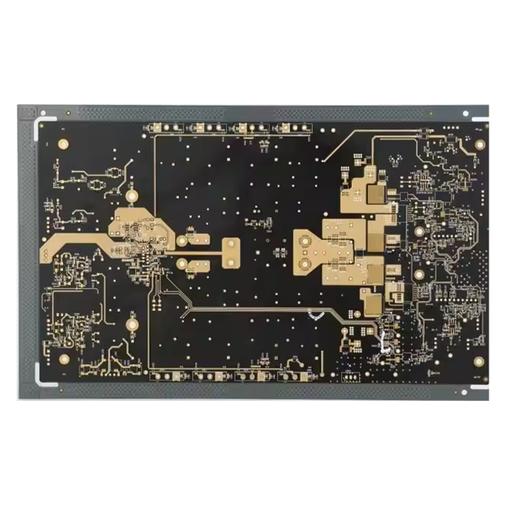
High-tech solutions such as antenna PCBs, PTFE PCBs, and multilayer PCBs distinguish themselves with superior performance in complex applications. These advanced PCBs leverage durable materials like FR4, providing excellent electrical insulation. For instance, the
High Tech Customized Antenna PCB, PTFE PCB, Multi layer PCB excels under extreme conditions due to its robust design, which also enhances its longevity and functionality.
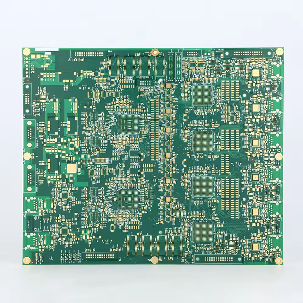
Advancements in multilayer PCB assembly have substantially improved quality and production efficiency, accommodating the growing complexity of modern electronics. The
New arrival Customized High quality Multilayer PCB assembly/PCB Manufacturer in China 3 utilizes high-quality FR4 material and customizable surface finishing to deliver excellent electrical performance while adhering to environmental standards.
Each of these products plays a significant role in pushing the boundaries of what's possible in PCB manufacturing, providing robust solutions for a range of complex, real-world applications.
Future Trends in PCB Manufacturing
The future of PCB manufacturing is leaning heavily towards sustainability, with manufacturers increasingly adopting eco-friendly practices. By utilizing environmentally-friendly materials and implementing waste reduction strategies, the industry is aiming to minimize its carbon footprint. These green practices not only address environmental concerns but also appeal to eco-conscious consumers, thus providing companies with a competitive edge in the market.
In addition, emerging technologies such as 3D printing and IoT integration are transforming PCB production. 3D printing allows for more rapid prototyping and customization, paving the way for innovative designs that were previously challenging or impossible to create. Furthermore, the integration of IoT in PCB manufacturing processes enhances connectivity and data management, leading to smarter, more efficient production systems that set new standards for innovation. These advancements indicate a trend towards more agile, adaptable production techniques that can keep pace with technological progress.
Conclusion
In conclusion, the PCB manufacturing landscape is undergoing significant transformations, spurred by key innovations and emerging trends. As the industry embraces eco-friendly materials and waste reduction strategies, it is evident that sustainability is not just a trend but a critical focus in future developments. The rise of technologies such as 3D printing and IoT integration paves the way for unprecedented levels of precision and connectivity in PCB production.
Looking ahead, the ongoing shift towards efficiency and sustainability promises to revolutionize how PCBs are designed and manufactured. With advancements aimed at reducing environmental impacts while enhancing performance, industry stakeholders are set to witness a new era of PCB technology. This trajectory not only underlines the importance of staying informed about technological progress but also emphasizes the need for manufacturers to adapt to these changes proactively.

 EN
EN
 AR
AR
 BG
BG
 CS
CS
 DA
DA
 NL
NL
 FI
FI
 FR
FR
 DE
DE
 EL
EL
 HI
HI
 IT
IT
 JA
JA
 KO
KO
 NO
NO
 PL
PL
 PT
PT
 RO
RO
 RU
RU
 ES
ES
 SV
SV
 TL
TL
 IW
IW
 ID
ID
 LT
LT
 SL
SL
 UK
UK
 VI
VI
 HU
HU
 TH
TH
 TR
TR
 FA
FA
 AF
AF
 MS
MS
 GA
GA
 HT
HT
 BN
BN
 LA
LA
 MN
MN