Full-process PCB design and manufacturing services are comprehensive solutions that cover every stage of producing printed circuit boards (PCBs). These services include everything from the initial concept and design phases to prototyping, testing, and final production. By offering a seamless workflow, they ensure high-quality outcomes and increase efficiency. Companies benefit from working with a single provider for all stages, reducing complexity and potential errors typically associated with transitioning between different service providers.
Integrated PCB solutions play a crucial role in enhancing operational efficiency. By allowing for optimized communication between design and manufacturing teams, such services also mitigate errors and streamline processes. For instance, industry leaders like MKTPCB and Alan Anderson Manufacturing exemplify successful implementations where their comprehensive services result in superior quality control and faster project turnarounds. According to Alan Anderson Manufacturing, their fully integrated services allow customers real-time tracking of their projects, significantly improving planning accuracy and efficiency.
In summary, adopting a full-process approach in PCB production not only elevates the quality but also optimizes the coordination across different stages of manufacturing, reflecting in improved time-to-market and customer satisfaction.
The PCB design process involves several crucial steps that ensure the successful development of printed circuit boards. First, conceptualization sets the foundation by defining the board's purpose and requirements. Next, schematic capture translates ideas into electronic representations, followed by layout design, where the physical arrangement of components is determined. Finally, design rule verification ensures the design adheres to industry standards. These steps benefit greatly from utilizing advanced software that supports industry norms and enhances design efficiency.
Choosing the right tools for PCB design is a vital aspect of the process. Popular software options like Altium, Eagle, and KiCAD offer specific features tailored to different project requirements. Altium is praised for its comprehensive design capabilities and robust library management. Eagle is often favored for small to mid-sized projects due to its user-friendly interface. KiCAD stands out with its open-source flexibility, making it a popular choice among engineers who prefer customization. Evaluations from tech blogs and user reviews frequently highlight these tools' effectiveness in simplifying design processes.
Full-process PCB services offer a holistic approach that spans from the initial design to the final production of printed circuit boards. This comprehensive service ensures a seamless workflow and guarantees high-quality outcomes by encompassing every stage of PCB development. As a result, companies benefit from integrated solutions that streamline communication and coordination between design and manufacturing teams.
The importance of integrated PCB solutions lies in their ability to enhance efficiency and reduce errors. By providing a unified platform for design and manufacturing, these services minimize miscommunications that often lead to costly reworks. For instance, industry leaders like Apple and Intel have successfully implemented full-process PCB services, demonstrating significant improvements in time-to-market and product reliability. These examples underscore the value of adopting an integrated approach in today's competitive manufacturing landscape.
Navigating the path from concept to creation in PCB manufacturing involves a series of intricate steps that demand precision and expertise. The journey begins with the careful selection of materials, where considerations such as material conductivity and thermal stability come into play. Subsequent fabrication techniques like etching, drilling, and layering form the physical structure of the PCB. These steps are complemented by assembly processes where electronic components are meticulously placed and soldered onto the board. Prototyping is crucial here, serving as a testing ground to uncover and rectify potential design flaws before full-scale production. By allowing for iterations and improvements, prototyping significantly reduces the risk of production delays.
Quality assurance in PCB manufacturing is indispensable to ensure that the products meet high reliability and durability standards. Implementing rigorous quality control measures, such as adherence to IPC standards and employing sophisticated testing methodologies like electrical and visual inspections, plays a vital role. Moreover, certifications such as ISO and RoHS compliance validate that manufacturing processes meet global standards, further assuring quality and safety. These measures collectively ensure that printed circuit boards are not only functional but also safe for usage in various technological applications.
Design for Manufacturability (DFM) is a crucial design philosophy that emphasizes collaboration among engineering disciplines to enhance manufacturability. By integrating considerations from various engineering fields early in the design process, DFM aims to streamline production and minimize potential issues. Key principles include simplifying designs, using standard components, and anticipating manufacturing challenges. This approach not only enhances product manufacturability but also fosters innovation and efficiency in printed circuit board (PCB) design.
Implementing DFM in PCB design offers numerous benefits, including reduced production costs, accelerated timelines, and improved product quality. By addressing manufacturability in the design stage, companies can avoid costly revisions and delays during production. For instance, a study demonstrated that a company reduced its production costs by 20% after adopting DFM principles. With DFM, businesses can deliver high-quality PCBs that meet or exceed customer expectations, thus enhancing their competitive edge in the market.
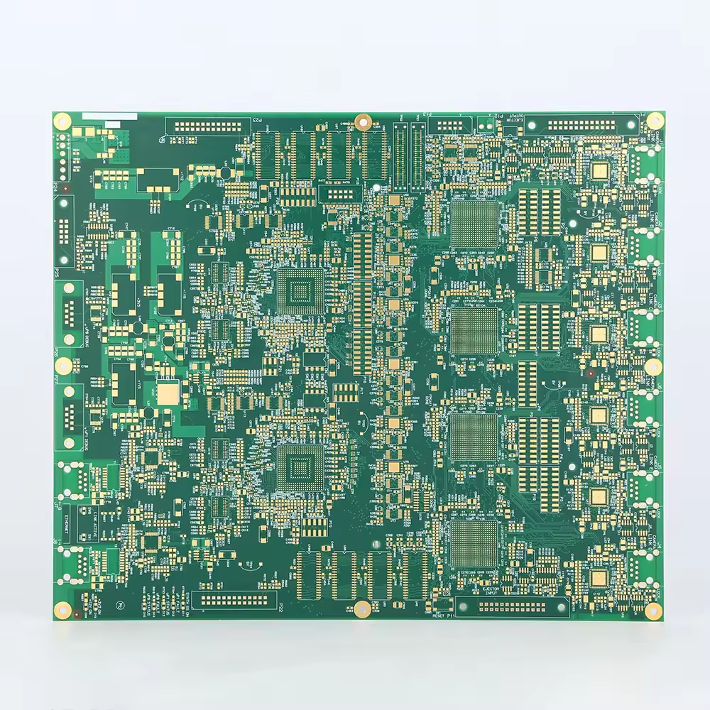
The process of PCB assembly has evolved significantly to meet the complexities of modern electronics applications. Various techniques, such as the High Tech Customized Antenna PCB, PTFE PCB, and Multi-layer PCB, play unique roles in these advancements. These boards are meticulously engineered with materials like FR4 and copper to enhance their electrical performance and robustness. For instance, the antenna PCB aids in high-frequency signal transmission, making it invaluable in communication technologies, while PTFE PCBs excel in applications needing stable dielectric properties under different environmental conditions.
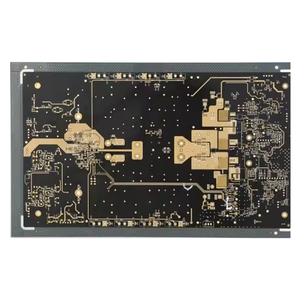
China is at the forefront of PCB assembly innovation, with companies consistently pushing the boundaries of quality and efficiency. The New Arrival Customized High Quality Multilayer PCB Assembly represents a leap forward in assembly technology, integrating cutting-edge manufacturing processes that ensure high performance and durability. Chinese manufacturers excel by leveraging advanced pick-and-place systems and automated testing solutions, establishing new benchmarks in the global PCB assembly industry.
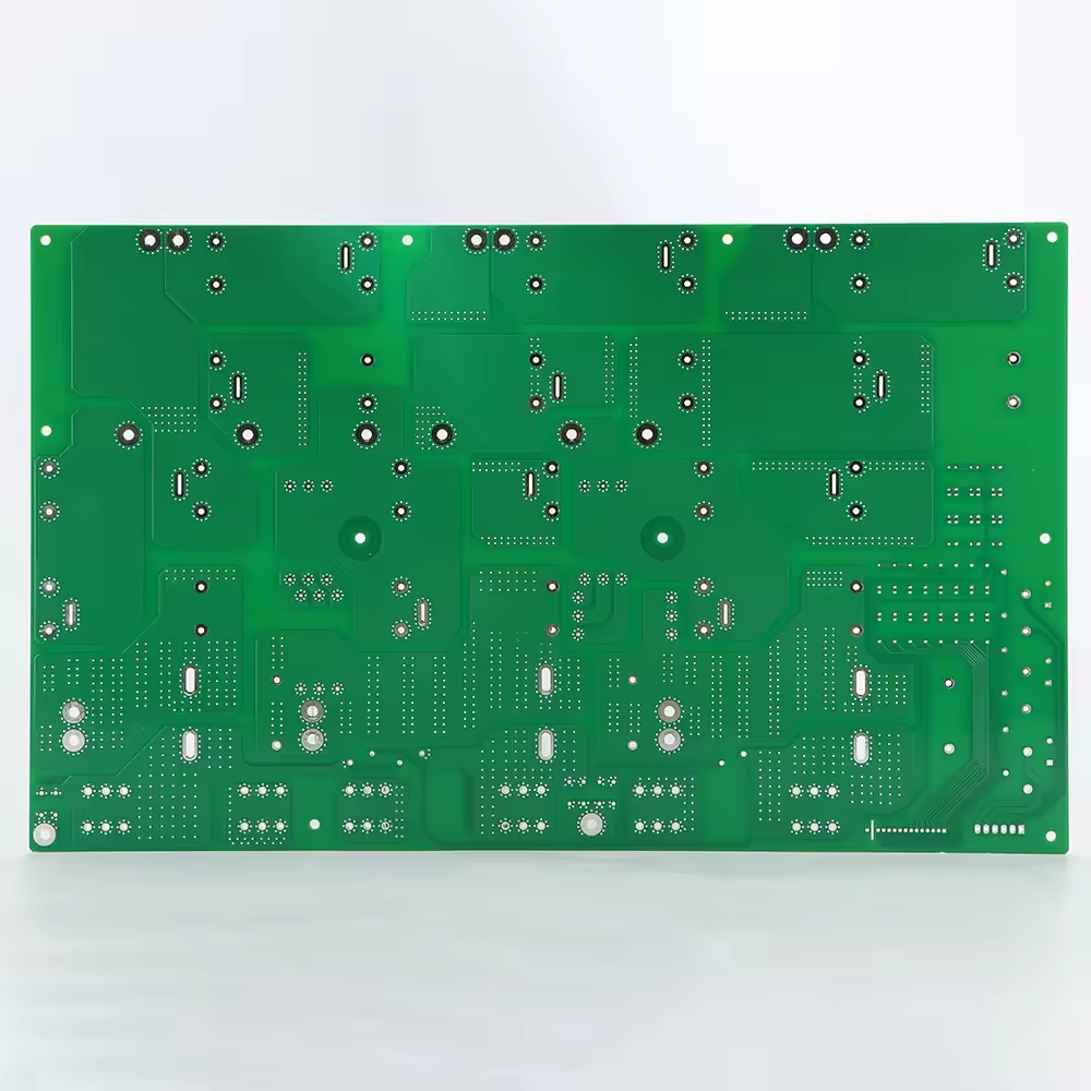
Furthermore, as illustrated by the New Arrival Customized High Quality Multilayer PCB Assembly 3, there is a competitive landscape among Asian manufacturers striving to deliver superior products. This competition drives continuous improvements in areas like layered designs and surface finish options, often complying with international standards to enhance global competitiveness. Such innovations not only bolster electronic efficiency but also align with environmental standards, showcasing the industry's commitment to sustainability.
Utilizing full-process PCB services offers significant cost efficiency and time-saving benefits. Engaging a one-stop service for all printed circuit board (PCB) needs can drastically reduce overhead costs and production times. For instance, consolidating design, manufacturing, and testing under one roof minimizes logistics and coordination expenses, which are often significant in multi-vendor setups. A study by the Global Electronic Design Automation Software Market highlights that streamlined processes contribute to efficiency, enabling faster market entry and reduced time-to-market for electronic products.
Another considerable benefit is the access to expertise that full-process PCB services provide. Working with a single provider offers clients the opportunity to tap into a deep pool of specialized knowledge, from printed circuit board design to manufacturing techniques. This breadth of expertise ensures that innovations are seamlessly integrated into the final product, enhancing both quality and performance. By leveraging the provider’s comprehensive insights into PCB materials and technology, such as advanced printed circuit board repair and manufacturing capabilities, clients can greatly improve their product’s competitiveness in the market.

 EN
EN
 AR
AR
 BG
BG
 CS
CS
 DA
DA
 NL
NL
 FI
FI
 FR
FR
 DE
DE
 EL
EL
 HI
HI
 IT
IT
 JA
JA
 KO
KO
 NO
NO
 PL
PL
 PT
PT
 RO
RO
 RU
RU
 ES
ES
 SV
SV
 TL
TL
 IW
IW
 ID
ID
 LT
LT
 SL
SL
 UK
UK
 VI
VI
 HU
HU
 TH
TH
 TR
TR
 FA
FA
 AF
AF
 MS
MS
 GA
GA
 HT
HT
 BN
BN
 LA
LA
 MN
MN

