With the advent of 5G technology, there is an increasing demand for printed circuit boards (PCBs) capable of supporting high-frequency signals. High-Density Interconnect (HDI) designs are crucial as they allow for the development of smaller, more complex circuits needed for compact electronic devices. These designs cater to the miniaturization requirements of modern electronics, facilitating efficient space utilization. Recent research indicates HDI technology can reduce board size by up to 50%, significantly enhancing space efficiency in dense electronic configurations. As industries progress towards more compact and capable devices, the role of HDI PCBs becomes indispensable, merging high performance with size constraints seamlessly.
In industrial settings, special PCBs designed for thermal management exhibit remarkable resilience to extreme temperatures, ranging from -40°C to +125°C. This capability makes them highly suitable for harsh environments where standard PCBs might fail. Incorporating thermal vias into these boards serves as an effective means to dissipate heat swiftly, thereby boosting device performance and reliability. As experts often stress, effective thermal management is crucial for extending the lifespan of electronic components. By ensuring consistent temperature control, these PCBs maintain optimal performance even under strenuous conditions, appealing to industries prioritizing durability and reliability.
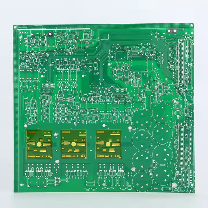
Specialized industries such as aerospace and medical sectors often demand unique PCB designs customized to meet specific application necessities. Such customization may involve selecting unique substrate materials, determining precise layer counts, or configuring distinct circuit patterns. Tailored solutions in PCBs are reported to improve operational efficiency by up to 30% for niche applications, according to industry statistics. This significant enhancement underscores the importance of bespoke PCB designs, which cater to precise performance and regulatory requirements inherent in specialized industrial sectors. By aligning with these unique needs, customized PCBs ensure optimal functionality and compliance in complex applications.
Material selection plays a crucial role in PCB performance, with FR4 being a common choice due to its cost-effectiveness and adaptability. However, for industrial-grade PCBs, FR4 might not meet the thermal and electrical demands of high-performance applications. Advanced substrates like Rogers or Polyimide significantly outperform FR4 in these domains, offering improved thermal management and signal integrity. Recent reports highlight that industries integrating advanced substrates can achieve a 20% increase in performance, showcasing the importance of substrate selection in optimizing PCB functionalities.
Implementing PCB V-Cut depanelizer techniques is essential for efficient PCB manufacturing, as these methods allow precise separation without compromising circuitry. Manufacturers benefit from reduced waste and heightened production efficiency, making V-Cut depanelizers attractive for sustainable processes. Usage statistics underscore their value, with firms utilizing V-Cut techniques observing up to a 15% increase in output. This focus on efficiency provides cost-effective solutions to meet the growing demand for PCBs in industrial applications.
Precision in microvia layouts and trace configurations is critical for high-density PCB designs, particularly for compact electronic devices. Microvias facilitate intricate circuit patterns that are necessary for optimizing space without sacrificing performance. The accuracy of trace layouts directly influences signal integrity, which is imperative for reliable PCB functionality. Industry standards dictate that trace widths must maintain a 5% tolerance to ensure robustness in crucial applications. Adhering to these specifications is vital for achieving optimal performance and reliability in industrial-grade PCBs.
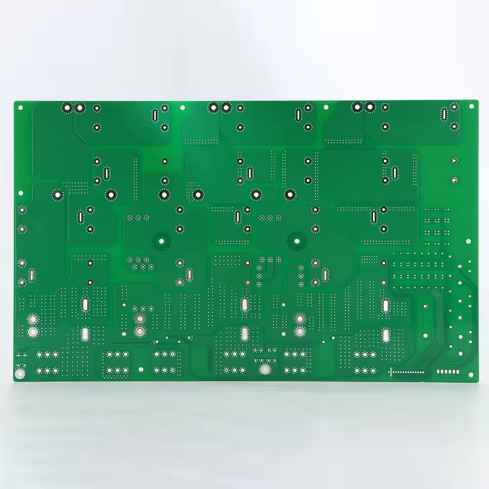
Multilayer PCBs are crucial in addressing the growing need for higher circuit density while ensuring continued functionality. Recognized manufacturers are leveraging cutting-edge technologies to fabricate these complex circuit assemblies, significantly enhancing their performance. For instance, a recent report indicates that adopting multilayer PCBs can effectively reduce a device’s footprint by up to 70%, providing a substantial advantage in compact electronic design. This makes them indispensable in applications that demand both miniaturization and robust performance.
Surface finishes play a critical role in the functionality and longevity of PCBs, particularly through enhancing solderability and preventing oxidation. Custom electronics PCB providers now offer a variety of specialized surface finishes, such as ENIG and HASL, to cater to specific application needs. This customization not only improves the electrical performance but also has been statistically shown to enhance the interconnect reliability of PCBs by 30%, proving vital in applications where robust connectivity is mandatory.
Rapid prototyping has transformed how companies validate and refine designs, significantly speeding up the product development process. Modern manufacturers now offer quick-turn PCBA services to address urgent market demands, maintaining a careful balance between speed and quality. This advancement allows businesses to reduce their time to market by an estimated 25%, thereby providing a competitive edge in rapidly evolving industries.
Implementing strict quality control measures is essential to ensure the reliability of PCBs in critical industrial applications. Techniques like automated optical inspection (AOI) play a crucial role in identifying defects early in the manufacturing process, thereby preventing costly failures. According to quality assurance statistics, companies with rigorous protocols experience up to 40% fewer failures, underscoring the importance of such measures in maintaining high reliability standards. PCBs used in critical applications must withstand harsh conditions, which necessitates stringent checks at every stage of production. This proactive approach not only assures the integrity of the PCBs but also enhances customer confidence and satisfaction.
Adhering to international certification standards, such as ISO 9001, guarantees manufacturing excellence and enhances the reliability of PCB products. Compliance with these standards increases customer confidence in the product's quality and enables PCB manufacturers to access broader markets. Industry reports highlight that adherence to globally recognized standards facilitates smoother international trade, enabling companies to expand their reach effectively. Following these standards also helps manufacturers streamline their processes, reducing production errors and contributing to higher product quality. Consequently, compliance becomes a strategic advantage in the competitive global market, ensuring that products meet the expectations of international consumers.
Long-term durability testing is essential for ensuring that PCBs can operate effectively under extreme conditions over their lifetime. Testing methods should simulate real-world operational stresses, such as thermal cycling and mechanical shock, to accurately predict product resilience. Studies have shown that durability testing can predict long-term reliability with over 85% accuracy, enabling manufacturers to improve their designs and materials for better performance. These tests help in identifying potential weaknesses before the product goes to market, thereby reducing the likelihood of failures under actual operating conditions. This rigorous approach not only mitigates the risk of product malfunction but also extends the PCB's operational life, making it a critical component of product development in industries where reliability is paramount.
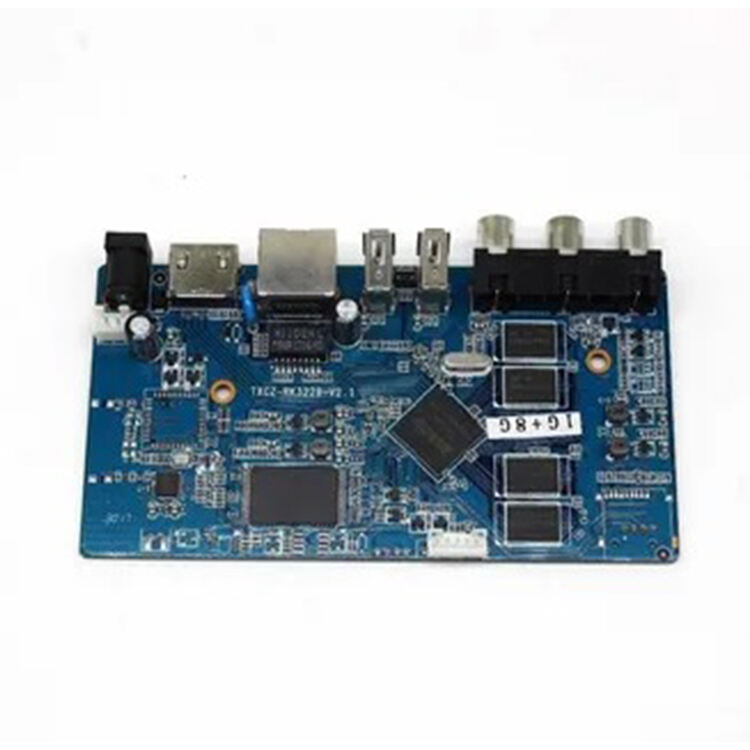
The increasing prevalence of the Internet of Things (IoT) demands printed circuit boards (PCBs) that facilitate connectivity and seamless interoperability. IoT-compatible PCBs are vital in integrating sensors and microcontrollers, allowing devices to communicate and interact effectively within an IoT environment. Innovative circuit designs are being developed to support these requirements, enhancing the performance of various electronic devices. Market analysts forecast that the demand for such IoT-compatible PCBs will see a remarkable growth of 30% over the next five years, driven by the surge in IoT device adoption worldwide. This growing trend highlights the transformative impact IoT will have on PCB manufacturing.
Substrate-like PCBs represent a major technological advancement in the industry, offering superior performance characteristics like reduced signal loss and enhanced thermal stability. Manufacturers are gravitating towards this technology to meet the demands of high-frequency applications, which require PCBs to operate efficiently without compromising on speed or signal integrity. According to industry reports, substrate-like PCBs can boost performance by up to 25% compared to traditional designs. This significant improvement is crucial as electronic devices become more complex and operate at higher frequencies. The adoption of substrate-like technology underscores a commitment to enhancing PCB manufacturing processes to cater to tomorrow's technological needs.

 EN
EN
 AR
AR
 BG
BG
 CS
CS
 DA
DA
 NL
NL
 FI
FI
 FR
FR
 DE
DE
 EL
EL
 HI
HI
 IT
IT
 JA
JA
 KO
KO
 NO
NO
 PL
PL
 PT
PT
 RO
RO
 RU
RU
 ES
ES
 SV
SV
 TL
TL
 IW
IW
 ID
ID
 LT
LT
 SL
SL
 UK
UK
 VI
VI
 HU
HU
 TH
TH
 TR
TR
 FA
FA
 AF
AF
 MS
MS
 GA
GA
 HT
HT
 BN
BN
 LA
LA
 MN
MN