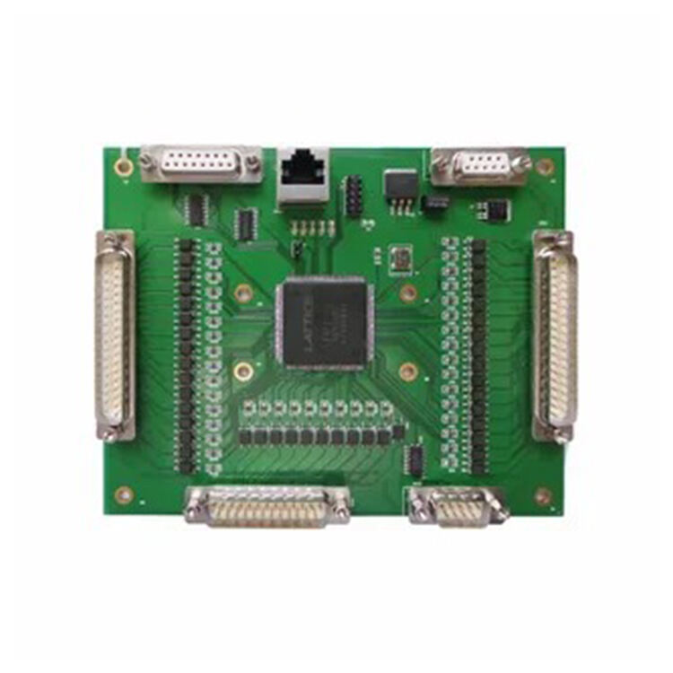
The PCB Assembly process is crucial in transforming raw components into functional electronic products. It involves several stages such as soldering, testing, and inspection to ensure quality. Various techniques like Surface Mount Technology (SMT) and Through-Hole Technology (THT) are employed depending on the design and complexity of the printed circuit boards.
Surface Mount Technology (SMT) has revolutionized PCB Assembly by enabling smaller, more efficient designs. SMT involves placing components directly onto the surface of a printed circuit board, which allows for higher component density and greater mechanical performance. Compared to traditional through-hole technology, SMT is preferred for its benefits in size reduction, increased functionality, and lower cost. Industry reports reveal that SMT is now used in over 90% of PCB manufacturing scenarios, emphasizing a clear shift towards this method due to its efficiency. Such widespread adoption is underpinned by its critical role in modern electronics production, where compact and fast-performing devices are in high demand.
Through-hole technology involves inserting components through pre-drilled holes on a printed circuit board, which are then soldered to pads on the opposite side. This method, while older, is still highly relevant in applications where components are exposed to mechanical stress, such as in industrial or automotive settings. Through-hole allows for more robust mechanical bonds, making it preferable in conditions demanding durability. According to industry standards, through-hole placement's reliability, especially in environments prone to vibrations and impacts, surpasses that of SMT. Its continued use in critical applications is a testament to its unwavering significance in ensuring strong and durable PCB assemblies.
Reflow soldering and wave soldering represent two predominant techniques in PCB assembly. Reflow soldering involves applying a solder paste to component leads and board pads, followed by a controlled heat source to melt the solder, creating connections. Conversely, wave soldering is used for through-hole components, where a wave of molten solder makes the connections. Reflow is often favored for its precision and suitability in mass production of SMT boards, while wave soldering is efficient for through-hole assemblies. Statistical data shows that reflow soldering is more widely used in industries requiring high-speed production of compact circuits, reflecting its adaptability to modern manufacturing needs.
Automated Optical Inspection (AOI) is essential for maintaining the quality of PCBs by identifying defects early in the production process. AOI uses advanced imaging technologies to detect issues such as misalignments, solder bridges, or missing components. By significantly increasing defect detection rates, AOI minimizes errors and boosts efficiency in PCB assembly lines. Case studies indicate that incorporating AOI protocols can enhance quality assurance processes, with some companies reporting a 98% success rate in defect detection and correction. This illustrates AOI's critical role in meeting high-quality standards, ensuring that only flawless products reach the market.
ODM (Original Design Manufacturer) and OEM (Original Equipment Manufacturer) are integral to the PCB assembly process, transforming design concepts into tangible products. ODM services offer the expertise to bring a complete and innovative PCB design to life, while OEM focuses on manufacturing products based on existing designs. These services improve product reliability and strengthen brand reputation by ensuring high standards and consistency in outputs. For example, renowned electronics companies leverage ODM/OEM services for efficient production and market presence, such as in consumer electronics and automotive industries.
Customized PCB layout services cater to specific application needs, enhancing performance and reliability in diverse environments. Designing PCBs requires consideration of several factors:
Successful layouts are evident in industries such as telecommunications and aerospace where precision is vital.
Sourcing PCB assembly from China offers substantial advantages, including cost-effectiveness and streamlined processes. Chinese manufacturers often provide one-stop services that consolidate production stages from design to assembly, simplifying the supply chain. This approach enhances efficiency, reduces lead times, and ensures consistency in product output. Market trends indicate robust growth in Chinese PCB manufacturing, attributed to technological advancements and quality standards, reaffirming the reliability of these services in industries such as consumer electronics and automotive.
Design for Manufacturing (DFM) is a crucial strategy that enhances the manufacturability and cost-effectiveness of PCB assembly. Essentially, DFM involves tailoring PCB designs to be easily manufactured while minimizing complexities and overall costs. By integrating DFM principles early in the design stage, manufacturers can anticipate production challenges and streamline the assembly process. Examples of DFM practices include optimizing component placement to minimize signal interference and designing for efficient thermal dissipation. These practices improve PCB quality by reducing defects and ensuring that the final product meets design specifications. A study by IEEE illustrates that DFM can lead to a significant reduction in production errors, highlighting its importance in maintaining PCB quality.
Selecting the right materials for PCB assembly is vital for ensuring longevity and optimal performance. Materials such as high-quality laminates and solder masks are essential in supporting the circuit’s mechanical and electrical requirements. Beyond material choice, effective thermal management plays a critical role in preventing failures, especially in high-performance circuits. Techniques such as using thermal vias and employing heat sinks can significantly mitigate the effects of overheating. Industry standards, like those from IPC, guide these material selections and thermal management strategies to maintain reliability in PCBs. Adhering to these standards can ensure that the PCB assembly withstands environmental stressors and operates efficiently over its intended lifecycle.
IPC standards are fundamental in maintaining high-quality PCB assembly by setting rigorous guidelines and specifications. Compliance with these standards ensures that PCB assemblies are reliable and market-ready. Certification, such as IPC Class 2 or Class 3, can enhance the marketability of PCB products by instilling confidence in their performance. The lack of adherence to IPC standards is directly linked to higher PCB failure rates; for instance, a report in Electronics Weekly noted that non-compliant assemblies had a 20% higher risk of malfunction. Therefore, ensuring IPC compliance not only boosts product reliability but also strengthens brand reputation and client trust.
The integration of IoT technologies into PCB designs represents a significant advancement in the field. As IoT aims to achieve seamless connectivity among devices, PCB layouts need to accommodate wireless communication components, creating a demand for innovative designs. This necessity leads to the use of advanced components and layouts that facilitate connectivity, influencing the entire manufacturing process. For instance, IoT-enabled devices such as smart home systems and wearable technologies exemplify how IoT demands compact yet highly functional PCBs. The evolving trend underscores the need for manufacturers to adopt cutting-edge design practices to keep pace with the growing market demands for IoT devices.
Innovations in automation technology are revolutionizing PCB assembly lines, significantly enhancing efficiency and precision. Automated systems are increasingly capable of handling complex assembly tasks with remarkable accuracy, reducing the need for manual intervention. This technological leap not only increases scalability but also ensures consistent quality in PCB production. According to industry reports, the trend is expected to accelerate, with forecasts suggesting a substantial rise in the adoption of automation in PCB assembly in the coming years. These advancements demonstrate the crucial role of automation in meeting the high demands for precision and volume in modern electronic manufacturing.

 EN
EN
 AR
AR
 BG
BG
 CS
CS
 DA
DA
 NL
NL
 FI
FI
 FR
FR
 DE
DE
 EL
EL
 HI
HI
 IT
IT
 JA
JA
 KO
KO
 NO
NO
 PL
PL
 PT
PT
 RO
RO
 RU
RU
 ES
ES
 SV
SV
 TL
TL
 IW
IW
 ID
ID
 LT
LT
 SL
SL
 UK
UK
 VI
VI
 HU
HU
 TH
TH
 TR
TR
 FA
FA
 AF
AF
 MS
MS
 GA
GA
 HT
HT
 BN
BN
 LA
LA
 MN
MN

