Double-sided PCB technology optimizes space utilization by accommodating components on both surfaces of the board. This design enhances the circuit density, crucial for compact devices like LED lighting and automotive dashboards. The core components of a double-sided PCB include substrates, copper layers, solder masks, and silkscreens. The substrate, often made of material like FR4, provides mechanical support, while copper layers conduct electricity. Solder masks protect the copper traces from oxidation and help with soldering, and silkscreens label components for easier assembly. The structure of these PCBs typically involves a dielectric layer sandwiched between copper layers to prevent electrical interference. This setup facilitates complex circuits without the bulk of multi-layer boards.
While single-sided PCBs have components on only one side, double-sided PCBs employ both surfaces, allowing for greater complexity and efficiency in circuitry design. This dual-layer approach offers a balance between complexity and size. Multilayer PCBs, with three or more layers, are used for highly complex circuits but come with increased production costs and intricacy. The advantages of double-sided PCBs over single-sided designs include more space-saving component placement at a relatively low cost. However, multilayer PCBs provide superior support for sophisticated devices requiring intricate connections but come with higher manufacturing complexity and costs. Thus, choosing between these types depends on the specific needs of the application.
Vias play a crucial role in circuit connectivity within a double-sided PCB by connecting the copper layers. These tiny holes facilitate the flow of electrical signals between the board's surfaces without adding substantial size to the PCB. There are different types of vias, including through-hole, blind, and buried vias, each serving unique purposes. Through-hole vias connect all layers and are common, while blind vias connect an external layer with an internal one without going through the entire PCB. Buried vias connect internal layers, offering more surface area for components on the external sides. The use of vias increases design complexity and impacts manufacturing processes, demanding precision in drilling and plating.
The manufacturing process of double-sided PCBs involves a comprehensive workflow that transforms initial design concepts into fabricated boards. This begins with the design phase, where engineers use specialized software to create the layout and circuit paths. Key steps in the process include:
Etching: Removal of unwanted copper from the board surface to engrave the circuit patterns.
Lamination: The bonding of substrates with copper layers which are vital for circuit formation.
Drilling: Precision drilling of holes for component placement and inter-layer connections.
Throughout these stages, the precise alignment of layers is crucial in preventing defects like misalignment and short circuits, which could compromise the PCB's functionality. The process requires keen oversight to ensure accuracy and reliability in the final product.
Plated Through-Hole (PTH) technology is a pivotal method in the manufacturing of double-sided PCBs, enhancing layer connectivity with superior electrical performance. PTH involves:
Drilling: Creating holes through both sides of the PCB.
Copper Plating: Coating these holes with conductive copper, facilitating electrical connections between layers.
PTH stands distinctly apart from methods like surface mounting by offering enhanced structural integrity due to the physical connection it provides. This technology is vital in establishing robust and efficient interconnections that are integral for maintaining the board's functionality, especially in complex and high-power applications.
Quality control is paramount in the PCB fabrication process, ensuring the reliability and performance of the final product. Critical measures include:
Electrical Testing: Verifying circuit continuity and resistance levels to detect potential defects.
Visual Inspections: Identifying physical flaws such as misaligned components or soldering errors.
Additionally, PCB manufacturing facilities adhere to certification standards like IPC standards, which define the industry criteria for various electrical properties and material specifications. These standards are crucial for consistent product quality and functionality, making them essential steps in the overall production workflow. The adherence to these standards ensures that every PCB meets the necessary durability and performance benchmarks.
The double-sided design of PCBs offers substantial enhancements in circuit density, allowing for more components in a compact area. This improved density leads to notable advancements in performance and reliability. For instance, studies highlight that the integration of double-sided PCBs in high-tech devices can boost operational efficiency by up to 30%. This high density is particularly advantageous in industries requiring compact designs, such as aerospace and telecommunications, where space is a premium and functionality cannot be compromised.
Double-sided PCBs are widely used in the automotive and consumer electronics sectors. In the automotive industry, these PCBs are integral to control modules, contributing to the development of smart cars by enhancing functionalities such as navigation and automated systems. Meanwhile, in consumer electronics, double-sided PCBs support compact designs essential for smartphones and tablets, aligning with market demands for lightweight and multifunctional devices. Industry projections suggest a growth trend of 5% annually in double-sided PCB usage due to increasing demand in these sectors.
Employing double-sided PCBs in power supply applications presents significant cost advantages. These PCBs efficiently use materials and advanced manufacturing techniques, reducing overall production costs. For example, through improved material efficiency and streamlined production processes, manufacturers report cost reductions of up to 20%. Such savings highlight the long-term economic benefits of double-sided designs, proving especially beneficial for projects with tight budgets and high-volume production requirements.
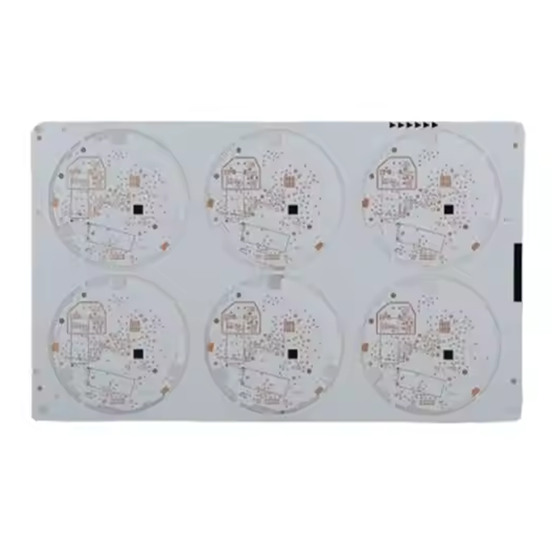
Aluminum core PCBs are a revolutionary development in solar lighting applications, offering exceptional heat dissipation. These PCBs are particularly beneficial for solar lighting systems due to their superior thermal conductivity, which enhances both durability and performance. Specific designs, such as those from ShenChuang's Solar Garden Light PCBs, are tailored to withstand outdoor conditions. These innovations in aluminum core PCBs have garnered industry recognition, with endorsements highlighting their efficiency and reliability in harsh environments.
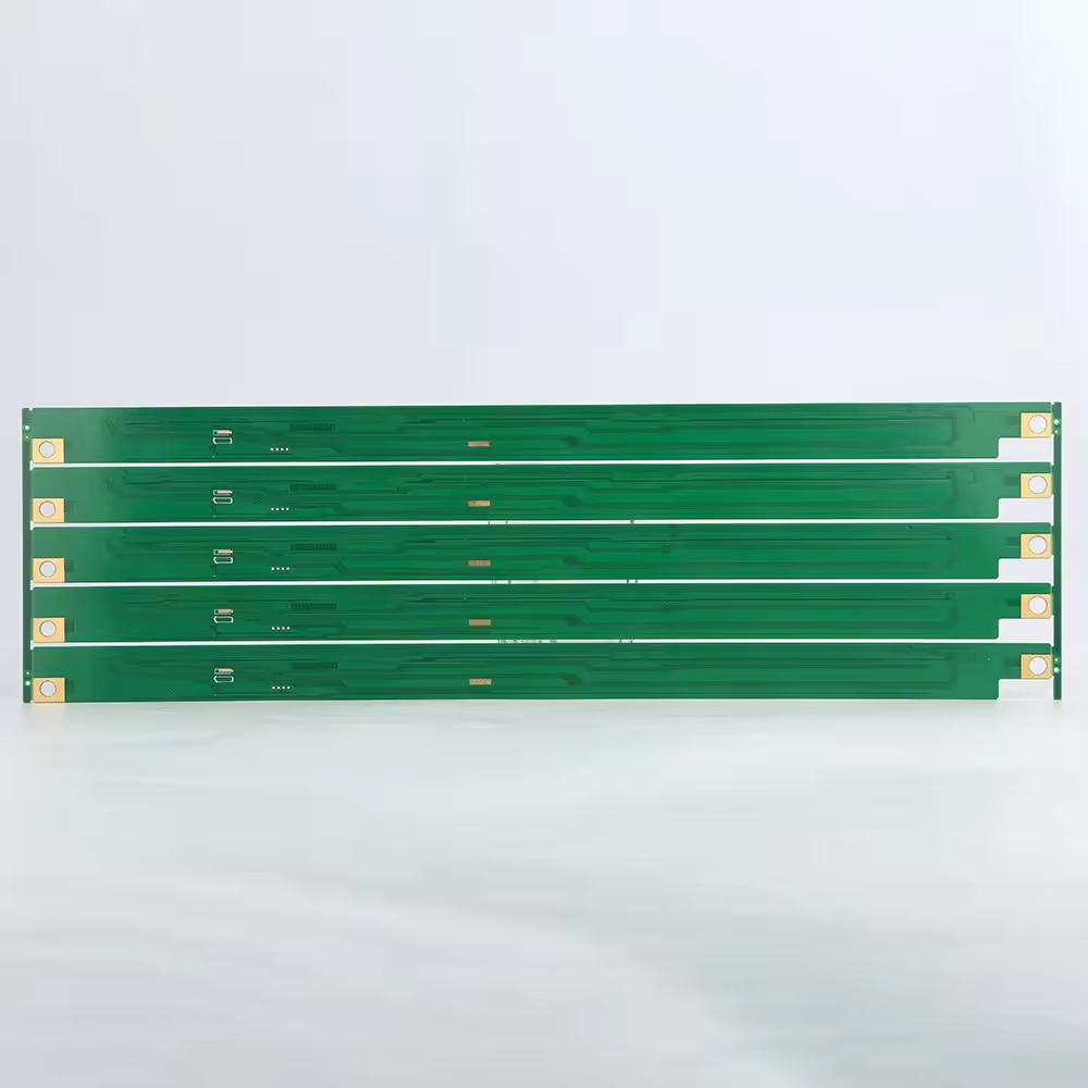
FR4 material stands as a cornerstone in high-performance PCB applications, particularly for double-sided configurations demanding reliability. This material's exceptional electrical insulation and stability make it ideal for environments requiring precision, such as telecommunications and aerospace industries. The advancements in FR4 technology have enabled more robust designs, meeting modern circuit requirements. As exemplified by ShenChuang's Multilayer PCB, these boards deliver reliable performance with enhanced mechanical and electrical properties.
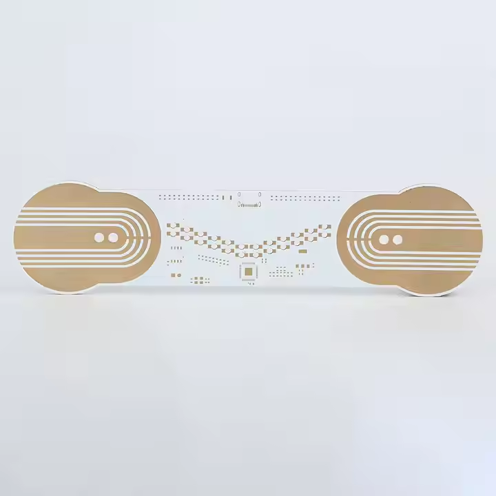
The trend toward customizable PCB configurations addresses specific industry needs, offering flexibility that enhances functionality. Tailor-made solutions such as ShenChuang's Double Sided PCB empower companies to innovate without limitations, perfectly fitting unique design requirements. This movement towards customized PCBs facilitates advanced applications and fulfills the growing demand for bespoke electronic solutions.
Effective thermal management is crucial in PCB design, ensuring long-term reliability and performance. Without proper strategies for dissipating heat, components can overheat, leading to failure or reduced lifespan. To combat this, designers employ several methods:
Heat Sinks: These are devices that absorb and dissipate heat from high-temperature components.
Thermal Vias: These are used to transfer heat between layers of the board efficiently.
Material Selection: Choosing materials with high thermal conductivity can significantly improve heat dissipation.
Research consistently shows that effective thermal management can extend the life of PCBs by preventing thermal fatigue, which is critical in high-density circuit boards like double-sided PCBs, widely used in LED lighting and power supply applications.
The choice of material in double-sided PCB construction significantly affects performance and durability. Common materials include FR4, known for being flame-retardant and cost-effective, making it ideal for high-performance applications. When selecting materials, consider the specific requirements of the application. For instance, flexibility is vital for PCBs used in wearable technology, while tolerance to temperature extremes is crucial for aerospace applications.
Studies indicate that high-performance materials can withstand harsh conditions, enhancing PCB reliability in demanding environments. Therefore, assessing material properties in conjunction with the intended application ensures optimal performance and durability, aligning with best practices in the industry.

 EN
EN
 AR
AR
 BG
BG
 CS
CS
 DA
DA
 NL
NL
 FI
FI
 FR
FR
 DE
DE
 EL
EL
 HI
HI
 IT
IT
 JA
JA
 KO
KO
 NO
NO
 PL
PL
 PT
PT
 RO
RO
 RU
RU
 ES
ES
 SV
SV
 TL
TL
 IW
IW
 ID
ID
 LT
LT
 SL
SL
 UK
UK
 VI
VI
 HU
HU
 TH
TH
 TR
TR
 FA
FA
 AF
AF
 MS
MS
 GA
GA
 HT
HT
 BN
BN
 LA
LA
 MN
MN